By Tim Williams
Introduction
One feature of the electronics industry that has become apparent, over the years of advising companies on EMC aspects of their designs, is the difficulty that many project managers seem to have in anticipating the problems that EMC requirements will cause to their project. Although it’s a universal feature – and you could say that an EMC consultant is going to bump into it fairly often, given his vocation – it seems to be especially prevalent in industries where large projects with detailed customer specifications are the norm. In such cases the requirements flow down from prime contractor to sub-contractor and further, and in so many cases, the understanding of what the requirements mean doesn’t flow down in parallel.
Many industry sectors suffer from this myopia: railway, automotive, telecom and aerospace are all affected. But the one which seems to suffer the most is the military sector. It has perhaps become more obvious in recent years, because of the squeeze on military spending, the expectation that the military should have access to the latest technology in the shortest timescale, and consequently the need to adapt commercial products for military use at the lowest cost – commercial-off-the-shelf (COTS).
In the EMC context, it works like this: the designer sees a functional requirement at the definition stage, and sees that it can be met by a commercially-available product. Along with the functional requirement, there is a whole stack of environmental requirements: such as shock and vibration, temperature and consequent heat dissipation, ingress protection, and of course EMC. The mechanical stuff is understood and can mostly be coped with, but EMC is a foreign country. They do things differently over there. As a result, the EMC requirements get pushed to one side in the early stages of project definition, with the expectation that they are simply an “engineering problem” that can be solved at a later date, if at all. There is a pious hope that when it comes to the scheduled EMC compliance test, the product will sail through without difficulty – or at least, any difficulties that arise can be offloaded onto someone else’s part of the system, or negotiated for a waiver, or at the most, dealt with by throwing in a few ferrites or filters, as one might apply a sticking plaster to a scratch.
The EMC consultant tends to get a phone call with an undercurrent of desperation when the EMC test has gone wrong and no such sticking plaster is obviously on the table. And this is, of course, the worst time to be involved in the project. Usually, the sales negotiators have bargained away any room for manoeuvre with the client. The most obvious engineering approach might be to find a sensible compromise between, for instance, discovered emissions that are “over the limit” and any expected susceptible frequencies in the eventual installation. (This is one implication of the “EMC Assessment” provision of the EMC Directive – one that’s never used, since product developers will go the extra mile, sometimes taking a company to the edge, to get that magic word “Pass” on the test certificate.)
Some standards – the US MIL-STD-461 is one of them – allow limits and levels to be tailored. Some users might want to “tailor” by reducing the severity of the requirement to meet the test result, which in some circumstances might actually be acceptable. But this is where the lack of understanding along the whole contractual chain is most pernicious. If a sub-contractor has signed up to meeting “the spec”, he can’t then renege on that, whatever the engineering practicalities, without substantial commercial penalties. And no project manager is going to put their career on the line for that.
COTS
A lot of the issues arise because commercial products – IT equipment, power supplies, instrumentation and so on – are pressed into service against EMC requirements they were never designed to meet. Or, as MIL-STD-461F puts it,
The use of commercial items presents a dilemma between the need for EMI control with appropriate design measures implemented and the desire to take advantage of existing designs which may exhibit undesirable EMI characteristics.
The use of commercial items presents a dilemma between the need for EMI control with appropriate design measures implemented and the desire to take advantage of existing designs which may exhibit undesirable EMI characteristics.
There has been considerable effort over the last few years to try and devise a way forward in such a situation. This has resulted in the concept of a “gap analysis”, in which the commercial specifications which a product is said to meet – usually under the CE Marking regime – are compared with the more stringent project specifications such as the military standards or the railway standards, and the identified “gaps” are filled by extra tests which may show the need for “mitigation measures”. Such a process has been described in for instance Cenelec TR 50538:2010, which works in the other direction – i.e. applying gap analysis to military equipment to prove that it meets the EMC Directive.
This process, while initially attractive, can fall at either of two hurdles:
- The product in question, despite its promises, doesn’t actually meet the detail of the specifications that it claims, or else it simply doesn’t claim enough of such detail to be useful. The CE Marking regime is so inherently lax that it would be surprising if it were otherwise;
- The “mitigation measures” which turn out to be necessary make the product unuseable in its intended application. For instance, the required extra filtering might double its size and weight, or the extra shielding might mean no-one could open the door to reach the front panel.
It may also be that the gap analysis simply isn’t able to identify all the gaps, which only eventually show up once the compliance test is done. Consequent delays to the project make it late and over budget, and the company ends up with the unhappily familiar project manager shuffle.
You might expect that companies which specialise in such projects would have learnt long ago of the dangers of postponing an analysis of EMC requirements, and indeed there are many such organizations that have EMC experts in house who can flag issues at an early stage. But there are also many who don’t, and even in the best organizations the in-house EMC specialist doesn’t always get the chance to offer the analysis that is required.
It doesn’t have to be like this. Some degree of early understanding of what the stringent specifications mean can save a lot of delay at the back end. Here are a few thoughts which come from a generalised fund of experience. Most of the issues arise from application of military standards to commercial products, so that will be the focus here: not to say that other areas don’t have their own issues, and some of these will also be mentioned. The two main military EMC standards are MIL-STD-461F in the US and DEF STAN 59-411 in the UK, and this article will look at their most common test requirements.
Power supply conducted emissions
Before we even get into high frequency issues, a lot of headaches arise at the low frequency end, particularly for AC power supplies. For large cabinet-mounted equipment, as in naval systems, it is common to try to use commercial power supplies, which have met EMC requirements according to the CE Marking standards. But military standards have a number of not-always-obvious requirements which conspire to trip the inexperienced.
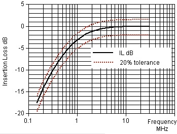
Supply harmonics: CE101
The first conducted emissions standard you come to is, in fact, mainly a limitation on supply harmonic currents: MIL-STD-461F CE101.
Image may be NSFW.
Clik here to view.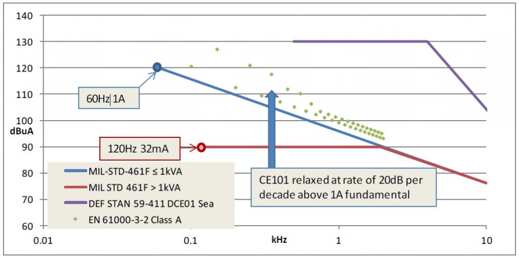
There are different requirements for aircraft and for naval applications. The above graph shows the CE101 limits for surface ships and submarines, alongside the UK DEF STAN limit for sea service, and the commercial Class A limits in EN 61000-3-2. The trick to understanding this is to see that different limits apply for equipment rated above and below 1kVA: and it’s counter-intuitive, in that more relaxed limits apply to the lower power rating. CE101 starts at the 60Hz fundamental and the harmonic limits are related to this value for equipment that takes more than 1A fundamental current, that is they become more relaxed for higher currents; but once your equipment takes more than 1kVA, suddenly the lower levels (adjusted upwards for actual fundamental current) kick in. For most electronic power supplies, this will mandate power factor correction.
Such a requirement is not unknown for commercial power supplies, and for European requirements at 50Hz, EN 61000-3-2 applies. But it doesn’t apply to 115V or 440V 60Hz supplies; and perversely, neither does it apply a limit to “professional equipment with a total rated power greater than 1kW”. And as can be seen from the graph, the 61000-3-2 limits are higher than the CE101 1A ≤ 1kVA limits.
The upshot of this is that if you know that CE101 will apply, make sure that the combination of all your specified power supplies can meet it – probably this will mean power factor correction on most of them. Don’t expect that a late change to do this will be easy – while it’s theoretically possible to apply a series choke at the input, any such choke will probably be bigger than the power supply itself.
Finally, notice that DEF STAN 59-411’s equivalent DCE01 requirement is much more relaxed, although as pointed out later, it uses a different LISN. But there are other military requirements which describe harmonic limitations, DEF STAN 61-5 and STANAG 1008 among them.
Supply harmonic limitations are related just to the AC supply frequency, and CE101 only extends up to 10kHz, though it will catch any other audio-frequency modulation or intermodulation effects on the supply. But then we get into the effects of the switchmode operating frequency itself.
Conducted RF on the supply: CE102, DCE01
Image may be NSFW.
Clik here to view.
Looking at the above graph, which compares the MIL-STD-461F CE102 basic curve (28V) requirement with the commercial CISPR Class A limit, firstly it’s clear that the CISPR limit is less stringent. In fact the MIL limit can be relaxed for higher supply voltages, and many supplies actually meet the CISPR Class B limit, which is around 10dB tighter; but on the other hand the CISPR limit applies the quasi-peak detector, which relaxes the measurement by contrast to the MIL’s peak detector. So a direct comparison is somewhat more complicated.
But the real issue is the extension of the MIL STD down to 10kHz. This is potentially devastating for the higher power commercial switchmode supplies whose switching frequencies are in the 20-150kHz range. Low power units generally have switching frequencies above 150kHz so that both the fundamental and its harmonics are controlled by the CISPR curve. There is normally no content below the fundamental, unless the emissions from several supplies with different frequencies are intermodulating. But commercial supplies with higher power and lower frequencies will not have applied filtering below 150kHz, because for their intended applications they don’t have to. (This is, in fact, a matter of some concern in the wider EMC context – see for instance Cenelec TR 50627:2015, Study Report on Electromagnetic Interference between Electrical Equipment/Systems in the Frequency Range Below 150 kHz).
This means that there will almost certainly be emissions below 150kHz which will be over the CE102 limit, and which may not be obvious from a commercial test report, which won’t show these lower frequencies. The identified mitigation measures would mean extra filtering on the supply input. But low frequency, high power filters are massive. Large chokes and large capacitors are needed. Space and weight penalties are inevitable.
That’s not the only problem: add-on filter design for frequencies of a few tens of kHz will encounter at least two other issues. One is earth leakage current. Capacitors to earth, to deal with common mode emissions, also cause supply frequency leakage. This can be a safety issue and also upsets earth leakage detection circuits, so there is usually a limit on the maximum capacitance that can be allowed. With regard to naval systems, MIL-STD-461F para 4.2.2 says
The use of line-to-ground filters for EMI control shall be minimized. Such filters establish low impedance paths for structure (common-mode) currents through the ground plane and can be a major cause of interference in systems, platforms, or installations because the currents can couple into other equipment using the same ground plane. If such a filter must be employed, the line-to-ground capacitance for each line shall not exceed 0.1 microfarads (μF) for 60 Hertz (Hz) equipment or 0.02 μF for 400 Hz equipment.
Then there’s the problem of filter resonance. A mismatch between an add-on filter and the existing filter in the equipment can create a resonance, typically at a few kHz, which actually amplifies the interference around that frequency. Rarely a problem for commercial products, it can cause unexpected difficulties when you are trying to meet low frequency emission limits: you put in a filter and it makes the emissions worse. To anticipate this, the best approach is to model the total filter circuit in a circuit simulation package such as Spice. But that requires knowledge of the filter component values, which is often not available.
The above comments apply particularly to MIL-STD-461F CE102. This measures voltage to the test ground plane across a 50μH LISN, just like the commercial test does, and so some comparison can be made. The UK DEF STAN 59-411 DCE01 test is different. It measures current to ground on each supply line, into a 5μH LISN. This makes a comparison with commercial standards harder. And, it covers a much wider frequency range: down to 500Hz (20Hz for aircraft), and up to 100MHz (150MHz for aircraft). The most stringent specifications are Land Class A or ship above decks, which apply a limit of 0dBμA (that’s 1 microamp!) from 1MHz (2MHz Land) to 100MHz. If you see this appearing in your specification, you can be sure that high frequency filtering requirements will be extreme; any switchmode noise, or microprocessor clock or data, cannot be allowed to get out into the power input. Careful mechanical grounding design as well as HF filtering and shielding of the supply will be essential.
Signal line conducted emissions
MIL-STD-461F does not have a test for signal line emissions. DEF STAN 59-411, on the other hand, does – DCE02. This is a common mode current measurement with the same limits as for the power lines, and it applies both to external cables and intra-system cables longer than 0.5m. If your cables are screened, then this test will exercise the quality of the screening; if there are any unscreened cables, then the interfaces to them will need to be filtered to prevent RF common mode noise. The test is not dissimilar to CISPR 22’s telecom port emissions test, but over a much wider frequency range and with a more universal application, not to mention generally tighter limits.
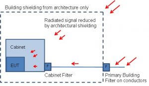
Although the US MIL STD doesn’t explicitly test signal line emissions, don’t make the mistake of thinking that the signal lines can therefore be ignored as a coupling path. They will contribute to radiated emissions and the radiated tests will pick these up. Whatever your test programme, the cable interfaces are a critical part of the overall test setup. One common error, having put a reasonable amount of effort into the design of the equipment enclosure(s), is to ditch all the good work by throwing in any old cable that comes to hand when the EMC test is looming. Always ensure that you are using, if not the actual cables that will be used on the final installation, at least a cable set that is equivalent in screening terms.
Radiated emissions
The military standards divide the radiated emissions requirements into two parts, for magnetic field and for electric field. Most of the commercial standards don’t: they only measure the electric field, from 30MHz upwards. There are some exceptions to this, which also measure the magnetic field below 30MHz, generally down to 9kHz. Certain lighting products under CISPR 15 are one example; marine equipment is another; and some users of CISPR 11 (industrial, scientific and medical) are also subject to this.
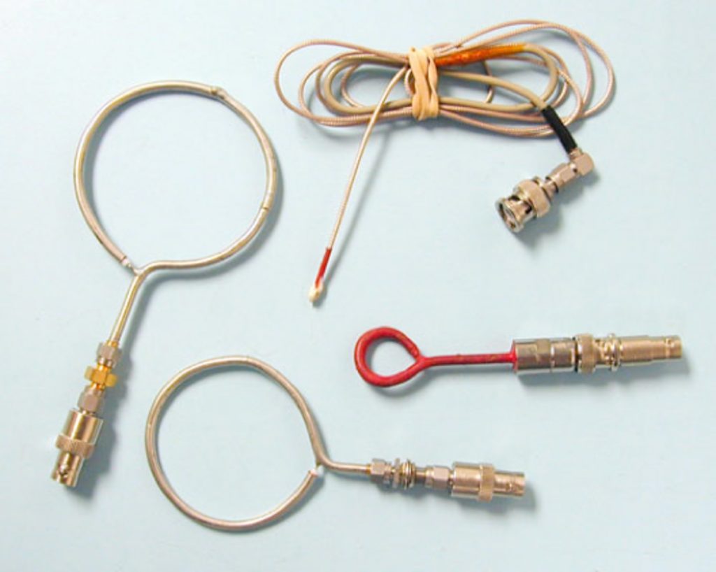
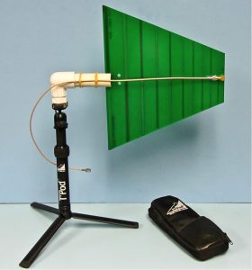
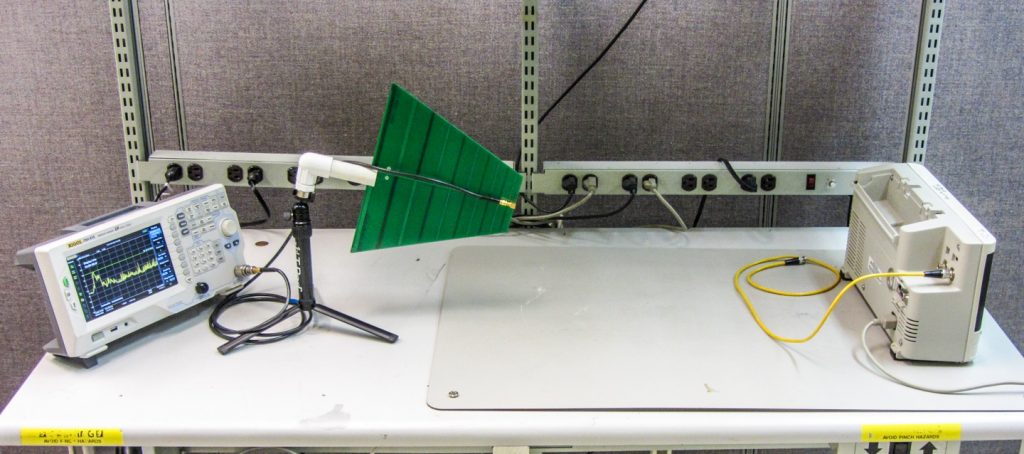
Magnetic field: RE101, DRE02
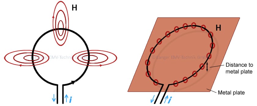
The military magnetic field emissions test is quite different from any other radiated test (except for the complementary magnetic field susceptibility test).
Image may be NSFW.
Clik here to view.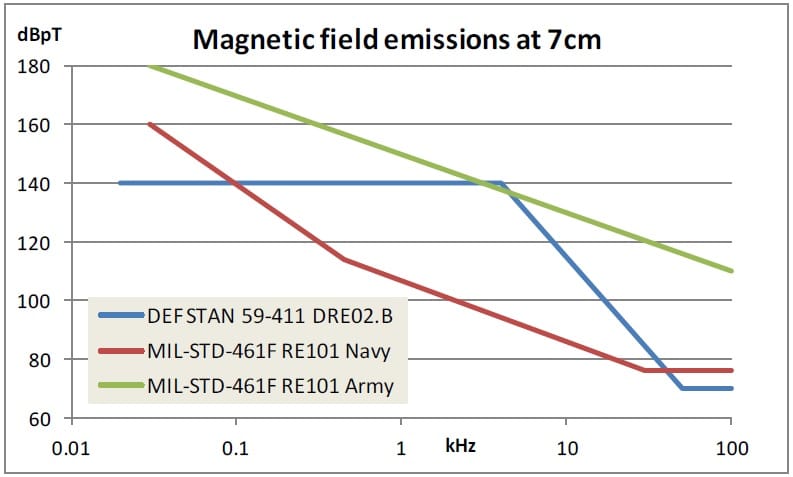
The method relies on a search coil being swept over the surface of the EUT to find regions of high field strength, and the field is then measured at a distance of 7cm from the surface. This method depends very much on the skill of the test engineer in finding the locations of highest emission. Both the UK DEF STAN and the US MIL STD use the same method, but their limits are different; for naval applications the MIL STD is generally more stringent, but otherwise the DEF STAN is.
The measurement is a test of low frequencies (up to 100kHz) in the near field. As such, the most likely sources will be magnetic components, particularly mains or switchmode transformers, or solenoids or motors, with high leakage flux. Commercial components almost never have to worry about emissions at these frequencies, so you will mostly have no handle on whether or not a particular component will actually be a threat, unless you do your own pre-compliance measurements in advance.
Mitigation measures in case of excess levels are fairly limited. Screening would require a thickness of magnetic material such as mu-metal or in milder cases, steel; occasionally a copper tape shorted turn around the outside of an offending magnetic core can help. If the emission can be traced to a particularly poor wiring layout – that is, high currents passing around a large loop area – then re-routing the wiring or using twisted pair will help. Otherwise, it’s a matter of finding an equivalent component with lower leakage flux than the culprit, or tackling the client for a waiver, based on the distance away from the EUT (greater than 7cm) where the unit does meet the limit.
Electric field: RE102, DRE01, DRE03
The military E-field measurement is more comparable to the well-known (in commercial circles) CISPR test, but only slightly. There are so many differences that a direct comparison of the two is really a mug’s game, even though in the context of gap analysis it would be highly desirable. We can visit the differences roughly as follows.
Physical layout, test distance and procedure
The CISPR test deliberately tries to ensure that the measuring antenna is in the far field of the EUT, with a minimum distance of 3m and a preferred distance of 10m – although the latter is not so common, given the much higher cost of suitable chambers that can accommodate it. This will indicate the interference potential of the EUT in the majority of commercial situations, when the vicitm’s antenna is well separated from the source. By contrast, the military and aerospace requirements place the measuring antenna at a fixed 1m from the EUT. The usual justification for this is that on many such platforms (aircraft, land vehicles and ships) the victim antennas are much closer. It also makes the measurement easier and, with low emission limits, aids in the fight against the noise floor of the test instrumentation.
It might be assumed that converting measurements from a far-field 3 or 10m to a near-field 1m, in order to directly compare a commercial result to a military limit, would be a simple matter of adding 9.5 or 20dB, on the assumption that the signal strength is inversely proportional to distance. In rare cases this might actually be true, but it certainly isn’t generally the case – the “conversion” factor can swing widely either side of this figure. So the default approach, using the above assumption, already introduces substantial errors. To understand why, you need to have a detailed insight into the electromagnetic field equations, which isn’t the purpose of this article.
Distance is just the start. The MIL-STD and DEF STAN test layout requires the EUT to be mounted on, and grounded to (if appropriate) a ground plane bench with its cables stretched out for 2m at a constant height of 5cm above the plane, before terminating in LISNs for power cables or in appropriate support equipment or the wall of the chamber, for signal cables. The CISPR radiated emissions test is different in every one of these aspects.
Image may be NSFW.
Clik here to view.
Image may be NSFW.
Clik here to view.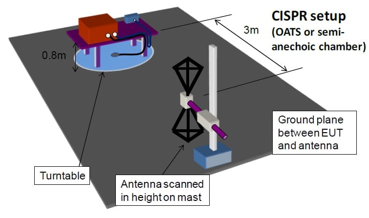
As well as this, the CISPR test requires the EUT to be rotated to maximise the emissions in azimuth. This isn’t a requirement of the military method, although it does leave open a requirement for maximization in orientation, without specifying how, other than “encouraging” the use of a pre-scan to identify the face of maximum emission.
Frequency range
The CISPR frequency range for radiated emissions starts at 30MHz and extends upwards to 1GHz or beyond, to 6GHz, depending on the highest internal operating frequency of the EUT. The military range is 10kHz to 18GHz, although not all applications require the whole range. Below 30MHz and above 6GHz there will be no data on commercial equipment performance.
Detector type and bandwidth
The military tests use the peak detector; the CISPR tests use quasi-peak (QP) for radiated emissions up to 1GHz, and peak above this. Both types give the same result on continuous interference signals but the QP gives up to 43.5dB relaxation to pulsed signals, depending on their pulse repetition frequency (prf). So, if a unit emits low-prf signals which rely on the QP detector to pass CISPR limits there will be a significant extra burden in converting these results to the military limits. To do so quantitatively, you would need to know the characteristics of interference sources at each frequency.
The measurement bandwidths are also different: 100kHz for the military standards from 30MHz to 1GHz, versus 120kHz for CISPR. Above 1GHz both use 1MHz. By comparison with other sources of error, the extra fraction of a dB potentially measured by CISPR below 1GHz is negligible and can be safely ignored.
Limits
In general, the CISPR limit lines are well established and for the majority of applications there are really only two sets: Class A and Class B, the latter being more onerous by 10dB and applicable to residential or domestic situations, Class A being applicable to nearly everything else. Military standards have many more variations depending on application, added to which the frequency ranges and levels can be modified by the customer’s contract. Because of these variations, it’s not generally possible to say that one set of standards is more or less onerous than the other, although it’s to be expected that any equipment mounted externally to the platform will have much more strict requirements than any commercial application. Additionally, DEF STAN 59-411 has a separate test, DRE03 between 1.6MHz and 30MHz (88MHz for man-worn equipment) – intended to mimic the use of equipment in close proximity to Combat Net Radio (CNR) installations used by the Army – which uses a tuned antenna representative of the Army’s radios. The antenna is “significantly more sensitive than the broadband antennas used in Test Method DRE01” and this allows even lower limits to be put in place for this application.
In summary, though, it is very difficult to make an accurate determination of whether a given piece of commercial equipment will meet military radiated emissions requirements through gap analysis. From the point of view of project planning, there are two principal coupling paths that radiated emissions will take from the equipment. One is radiation directly from the enclosure, the other is radiation from cables connected to the enclosure. Therefore, areas of the design that need the most work to control these emissions will include cable screening and enclosure screening. The more critical the limit levels – and the wider the frequency range – the more important it is to actively design the enclosure for screening effectiveness; and also to ensure that cable and interface construction maintains the screening effectiveness. The two areas are complementary, one will be useless without the other. Conductive gaskets for seams and connector shells in the enclosure need to go hand in hand with selection of screened cable and termination of that screen to the mating connector. The trick lies in understanding that here we are dealing with the electrical performance of mechanical components, and so both areas of design must be evaluated.
Marine equipment
Before leaving the subject of limits, one non-military application where it is possible to apply a gap analysis is in radiated emissions of civil marine equipment. The marine standard IEC/EN 60945 uses substantially the same method as the normal CISPR tests and CISPR results can be compared, almost directly. It would be quite typical to want to use CISPR Class A-compliant equipment – such as video monitors or network switches – on board a ship. The two limits are compared below. Note that over much of the frequency range the marine requirements are quite relaxed. But there’s one exception: the VHF marine band, 156-165MHz, where they are anything but relaxed. This can cause substantial headaches for marine system builders, and it’s as well to be aware of this at the outset.
Image may be NSFW.
Clik here to view.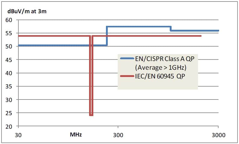
RF susceptibility
Radiated
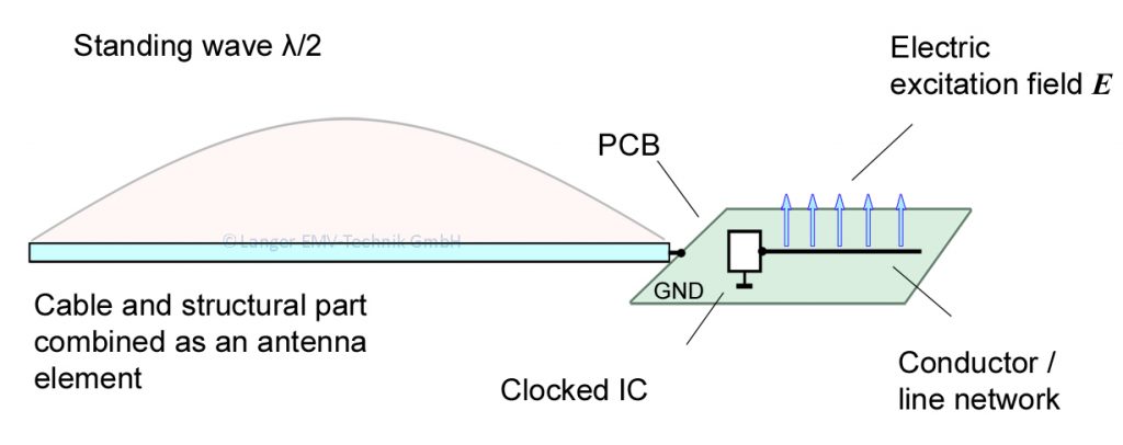
The coupling routes for radiated RF susceptibility issues are generally the reciprocal of those for radiated emissions, and therefore shielding design techniques will work in both directions. However, the internal circuits which are affected by high level applied RF fields may be quite different from those which create emissions. It is usual for power switching circuits and digital processing to create RF emissions while being relatively unaffected by incoming RF; in contrast, low-level analogue circuits, typically for transducer or audio processing, will not create emissions but may be affected by millivolts of RF. Therefore for many products there can be different areas which are relevant for one or other phenomenon.
Applied RF field levels, as with emissions limits, can show wide variations depending on the required standard and application. DEF STAN 59-411 DRS02 has a “Manhattan skyline” of levels versus frequency, ranging from typically 10V/m at low frequency to 1000V/m, pulse modulated, in the microwave region, if equipment will be sited potentially in the main beam of a radar transmitter (2000V/m for aircraft). MIL-STD-461 RS103 has a rather more uniform set of requirements, ranging from 10V/m for ships below decks to 200V/m for aircraft. RTCA DO-160, which is widely applied for civil aircraft equipment and often for military ones too, has a massive table (rather than a Manhattan skyline graph, but to the same effect) which defines susceptibility levels versus frequency for 12 different categories of equipment, with the least severe being 1V/m and the most severe being 7200V/m. Frequency ranges are tailored to the application as well, but can extend from 10kHz to 40GHz.
Compare this to the majority of commercial standard requirements, which are generally fixed at 3V/m for residential and 10V/m for industrial and marine applications; railways push the boundary to 20V/m, and the basic standard IEC 61000-4-3 proposes a maximum of 30V/m. And the frequency range for these radiated requirements starts at 80MHz and goes up to 2.7GHz at the most, with much lower levels being the norm above 1GHz; it may be fair comment that most commercial products aren’t expected to find themselves in the main beam of a surveillance radar. (It’s noteworthy that the commercial tests refer to immunity, whereas the military/aerospace ones refer to the same phenomena as susceptibility.)
Relating these levels means that the more stringent specifications will demand a high degree of extra shielding, which has to be allowed for in the initial design choices. Trying to add or improve shielding later in the mechanical design is always going to create serious headaches.
Test method
As with radiated emissions, there are differences in the susceptibility test procedure too. The military test layout stays constant between emissions and susceptibility. The CISPR/IEC layouts are different, much to the chagrin of test labs who have to re-position equipment between tests and sometimes use different chambers in order to maintain compliance with the specifications. But for the radiated susceptibility test, the biggest issue lies in how the field strength is controlled. For the tests in MIL-STD-461 and DEF STAN 59-411 (but not DO-160) the applied field strength at a probe near to the EUT is monitored and controlled during the test. For DO-160 and the commercial test to IEC 61000-4-3, the field is pre-calibrated in the absence of the EUT and the same recorded forward power is replayed during the test. These two methods can produce fundamentally different results, for the same specification level in volts per metre, depending on the nature of the EUT.
In addition to this, there are differences in the modulation that is applied to the RF stress. The military and aerospace tests prefer 1kHz square wave modulation, but also pulse modulation where it is relevant (at radar frequencies), along with other more specific types of modulation in some cases. The IEC 61000-4-3 test uses only 1kHz sinusoidal modulation; but it does require 80% modulation depth, which effectively raises the peak applied stress level to 1.8 times the specification level. In this narrow sense, the commercial test is more stressful than the military, for a given spec level.
But when you are looking at a test report for a COTS product, for any immunity test one of the most important questions is: how was the product monitored during the test, and what criteria were applied to distinguish a pass from a fail? In many test reports, this information is so vague as to be of no help whatsoever, yet it is actually what determines the suitability of that equipment for the application. No test standard will specify the performance criteria in detail; that is the job of the test plan for that product. The report should reference the test plan and where necessary reproduce its detail. Few commercial test reports do this – often, one suspects, because there never was a test plan in the first place.
Conducted RF
Similar issues apply to the specifications for conducted RF susceptibility. Direct comparisons are harder because commercial standards, based around IEC 61000-4-6, apply a voltage level to the cable from a source impedance of 150Ω; virtually all other standards use the method of “bulk current injection” which applies a current level via a clip-on current transformer. Relating the two is only possible if you know the common mode input impedance of the interface you are testing. It would be fair to say that even the designers most familiar with their product will be guessing – it’s not a feature which is necessary to know for the functioning of the equipment, even though it has a direct impact on EMC performance.
Beyond this, as with radiated RF susceptibility, the military and aerospace requirements have a smörgåsbord of levels versus frequency for different applications. DO160 has a maximum of 300mA, MIL-STD-461 CS114 has 280mA and DEF-STAN 59-411 DCS has 560mA for their most severe applications. If we take the power into the 50Ω calibration jig, this is between 4 and 15 watts. Compare this with the typical 10V emf from 150Ω which gives 5Vrms into a 150Ω calibration, as required by IEC 61000-4-6, which is only 166mW.
Design mitigation measures for this test are limited to two principal approaches: effective screening of cables, and effective filtering of interfaces. One can possibly substitute for the other, but a combination of both is the best method. Any weakness in cable screen termination will allow interference through to the screened circuit within, which can be mopped up by a moderate degree of filtering. The overall protection, though, must work across the frequency range of 10kHz to 400MHz (200MHz for MIL-STD-461). Designing a filter which will deal with this spectrum, even for power supplies, is not trivial and usually the most cost-effective approach is the combination.
Lightning and transient susceptibility
The US MIL-STD-461 doesn’t have an explicit lightning surge test, at least up to issue F. One is under discussion for issue G. The UK DEF STAN 59-411 does have some serious surges, including one for lightning (DCS09), but the most comprehensive is that in section 22 of DO-160. This has been uprated in every re-issue of the standard and is now one to challenge any aircraft equipment designer – if, that is, you can decode the arcane instructions for how to select the various levels and waveforms.
This author was privileged to visit the lightning surge test facility of a major Chinese telecomms supplier a few years ago (the capacitor bank alone filled most of the room – “Please, Mr Tim, make sure to stand well back when I press this button”) – there are regions of the world where thunderstorms are the norm rather than the exception, and telecom towers are natural attractors for the strike. So some parts of the facility had to be tested with the full whack. Aircraft, naturally, can’t be trusted not to fly near to or even under (not into) a thunderstorm occasionally. But practically, the test levels need to be tailored more to the currents that would be expected on the wiring interfaces, which in turn depends on the unit’s location in or outside the aircraft, the level of hardening required and the type of construction of the aircraft’s structure.
DO-160 version G has two methods in its section 22: pin injection, and cable bundle tests. The first is a “damage tolerance” test; the second evaluates “functional upset tolerance” and has a variety of waveforms including single and multiple stroke and multiple bursts. The best commercial equipment may be specified to cope with the IEC 61000-4-5 lightning surge test, but this does not include pin injection, and its surge waveform does not reflect the variety of waveforms required by DO-160. Extra interface protection will be needed if you are trying to use such equipment in this application.
Pin injection
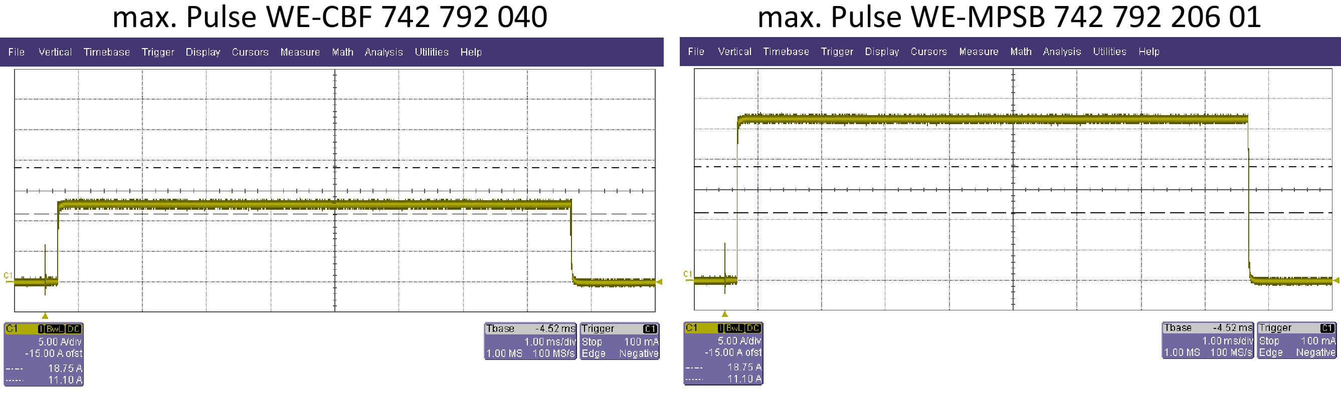
For this type of test, the EUT needs to be powered up and operating, but its connectors (except for the power supply) are disconnected and the specified transient pulse is applied, ten times in each polarity, between each designated connector pin and the ground reference. Thus cable screening is of no relevance for this test. If the power input is to be tested, the transient is applied in series with the supply voltage, with the external supply source properly protected.
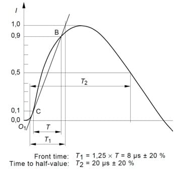
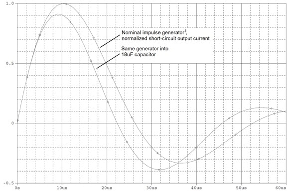
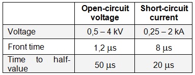
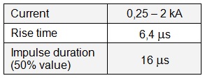
Three different waveforms are specified, with five possible levels. The most stressful in energy terms is waveform 5A, which is a 40/120μs surge with a 1Ω source impedance and a peak voltage from 50V (Level 1) to 1600V (Level 5 – this one is fairly rare, but level 4 at 750V is not uncommon). The other waveforms (labelled 3 and 4) are a 1MHz damped sinusoid and a faster unipolar transient, from higher source impedances.
Cable bundle
These tests are intended to check for both damage and upset, and work by injecting transients into each cable interface as a whole, either via a current probe or by a connection between the unit enclosure and the ground reference of the test. In this case, cable screening effectiveness is crucial. In a well-screened system the surge will pass harmlessly down the cable screen and around the EUT enclosure without impinging on the inner circuits. Successfully beating this test then means ensuring that both the cable assembly and the enclosure have a low transfer impedance, to prevent common mode currents developing internal voltages. To put a sample figure on this, a transfer impedance of 50mΩ/m, typical of a good quality single-braided screen at 10MHz, when faced with a 1000A surge down the screen, will create a 50V pulse in common mode on the cable’s internal circuits per metre length. A double-braided screen could drop this to 1mΩ/m and hence 1V. But that demands extreme care in assembling the connector screening shell.
Alternatively, if a cable is unscreened, the interface has to absorb or resist the injected surge in the same way as for pin injection. And in addition, the unit has to continue operating without upset, so any pulse propagating into the circuit must not affect its operation.
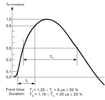
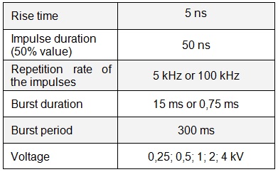
The cable bundle tests use the same waveforms (3, 4 and 5) as before, with possibly two more, waveform 1 being the current equivalent of waveform 4 (6.4/69μs) and waveform 2 being a faster one with 0.1μs risetime. Single stroke, multiple stroke (one large plus thirteen smaller transients) and multiple burst (three bursts of 20 damped sinusoid transients, every 3 seconds, for at least 5 minutes) application are specified. Waveform 6 applies to low impedance cable bundles in place of waveform 3 for multiple burst tests. The levels vary from 50V/100A for the mildest to 1600V/3200A for the most severe, and that’s just for waveform 1.
Transient protection
Given that your specification, once it has been decoded, will be quite explicit as to the levels and pins to be tested, you can design in protection with a good knowledge of what it will be protecting against. There are two main techniques. The first is isolation: if all interfaces are isolated from ground, and the isolation barrier can withstand the full surge voltage, this is a good start. But remember that there is a dv/dt associated with the surges and therefore capacitance from each circuit to ground and/or through the isolation barrier is also important, since the edge of the stress waveform will be coupled through this capacitance to the circuits. If you are relying only on isolation, it is necessary to identify parasitic and intentional capacitances to the ground reference (usually the enclosure) and make sure that the paths these provide are innocuous.
The second method is clamping the surge voltage with transient suppressors to ground. Since energy will be deposited in the suppressor on each test, you need to size it appropriately for the specification level to be sure it is not over-stressed. You also need to be sure that the downstream circuits can withstand the peak voltage that the suppressor will clamp to. Whilst they can be effective, suppressors aren’t suitable for all types of circuit, particularly wideband interfaces. And complementary to the comment above on capacitance, when a suppressor clamps a transient, it passes a di/dt current pulse; any inductance in series will create a secondary transient voltage, from V = -L·di/dt, which may be at damaging levels. Short leads and tracks, going directly to the right places (perhaps the enclosure, perhaps local circuit nodes) are critical.
Another more sophisticated approach is to block the surge path but only during its actual occurrence, using a series-connected high voltage MOSFET and control circuitry. Given the relatively slow risetime of the waveforms this is feasible, but it is complex, and has to take into account both surge polarities. It may well be necessary in high-reliability applications when you simply cannot use a transient suppressor, because if a suppressor is destroyed open-circuit this will not be apparent – the equipment will carry on operating normally – but you will have lost surge protection without knowing it. (A related question is, is it better for a transient suppressor to fail open circuit or short circuit? It could fail either way, but the consequences are wildly different.)
Equipment categories
The actual tests and levels applied depend on the application and need to be clearly specified in the procurement documentation. This should be “consistent with its expected use and aircraft installation”. The specification should consist of six alphanumeric characters as shown below. The first, third and fifth letters are “waveform set designators”, determining which tests are to be done with which waveforms – decided by the type of aircraft and whether or not the cables are screened – and the other numbers n, i and j apply levels for each set of tests, depending on where in the aircraft the equipment will be mounted.
Image may be NSFW.
Clik here to view.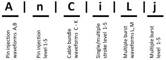
X in the specification means no tests are to be performed, Z means that the test is performed at levels or with methods different from the standardized set.
As a very, very approximate first pass judgement, the higher the numbers and the further into the alphabet go the letters, the more severe is the test. But you can see that the complexity is daunting and every case has to be analysed in its own right.
Other transient tests
By comparison with DO-160 section 22, other military transient tests are fairly straightforward, although not necessarily lenient. In most cases the transients are applied by current probe on cable bundles; this is the case for MIL-STD-461 CS115 and 116, and for DEF STAN 59-411 DCS04, 05, and 08. DCS06 is applied on power supply lines individually, as is also DCS08. The nearest test to the DO160 lightning tests is DEF STAN 59-411 DCS09, which applies similar and in some cases identical waveforms. A wry note at the beginning of DCS09 says
When testing with the Long Waveform, in particular, it is advisable for personnel in the vicinity of the EUT to wear eye protection. Some components have been known to explode and project debris over distances of several metres. Some types of pulse generators can produce a high intensity burst of noise when they are fired. Operators, trials engineers and observers should be made aware of this and advised to wear ear protection.
Transient suppressors, where they are used, should be sized appropriately.
Supply voltage ratings
As a final piece of light relief, don’t forget that some equipment specifications make substantial demands on the power supply’s robustness. We’ve already mentioned harmonic current limits at the beginning of this article, but there are other power input issues which do, strictly speaking, fall under the umbrella of EMC. They don’t appear in MIL-STD-461 or DEF STAN 59-411, but there are other military requirements which are relevant, for instance MIL-STDs 704 and 1399, or DEF STAN 61-5, or STANAG 1008. RTCA DO-160 for aerospace has section 16 (which does include harmonic current limits); and in another industry, railway rolling stock equipment has to meet EN 50155. Mostly, these specify the degree to which input voltage dips and dropouts can be expected, along with the levels of under- and over-voltage in normal and abnormal operation. The last of these is often the most stressful.
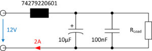
DO-160 section 16’s abnormal over-voltage requirement for Category Z (the most severe) on 28V DC supplies demands that the power input withstand 80V (+185%) for 0.1 second and 48V (+71%) for 1 second. Even the least severe, Category A, requires +65% for 0.1 second and +35% for 1 second. For EN 50155, a voltage surge on a battery supply of +40% for 0.1 second should cause no deviation of function, and for 1 second should not cause damage. Overvoltages for such durations can’t be clamped by a transient suppressor; suppressors, if used, need to be rated above the peak voltage that will occur for these conditions. But at the same time, it can be difficult to design power supplies for such levels using conventional SMPS integrated circuits. Instead, a discrete pre-regulator – which might also implement other functions such as soft start and reverse polarity protection – is a common solution. So the complete power supply input scheme for a DC supply is likely to look like that shown below, and the early components need to be substantially over-rated compared to the normal operating voltage.
Image may be NSFW.
Clik here to view.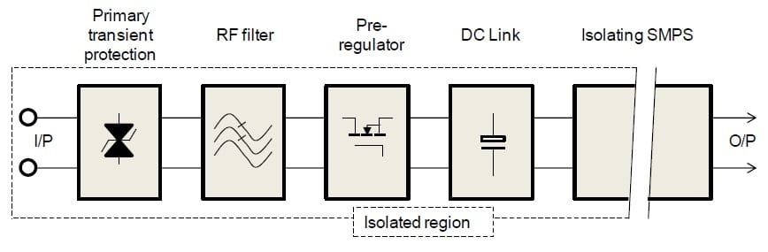
Conclusion
With all the above requirements, limits and levels in mind, if you are expecting to use any commercially-produced apparatus within a system that needs to comply with military/aerospace requirements, or others for which it wasn’t designed, it should by now be obvious that right at the beginning of the design process, you must start with a detailed review of the procurement contract’s EMC specification before you get involved in any negotiations on contract price. EMC requirements have the potential to make or break a project – they must be respected and their implications for schematic, PCB and mechanical practices understood.
Tim Williams
Elmac Services
May 2015
www.elmac.co.uk
mailto:consult@elmac.co.uk


![Vermillion_Fig4]](http://www.interferencetechnology.com/wp-content/uploads/2016/04/Vermillion_Fig4-300x106.jpg)